MAKE A MEME
View Large Image

| View Original: | CMOS OR.svg (300x200) | |||
| Download: | Original | Medium | Small | Thumb |
| Courtesy of: | commons.wikimedia.org | More Like This | ||
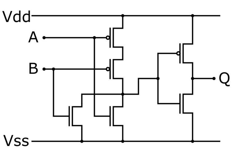
| Keywords: CMOS OR.svg ValidSVG made with Inkscape Layout of NMOS and PMOS components in an OR Gate This OR gate is implemented as an AND gate with both inputs inverted by using PMOS at the top as well as the otutput inverter at the right which is functionally correct but is not commonly used as it requires 2 extra transistors Own drawing Inkscape 0 43 12/07/06 inductiveload PD CMOS | ||||